
Spectrum Logic has developed CMOS X-ray detectors designed for semiconductor packaging, where devices and sensors are integrated into compact architectures to improve performance and efficiency. Examples include graphics processing units (GPUs), high bandwidth memory (HBM) and multi-layer ceramic capacitors (MLCCs)—a type of surface-mount capacitor that also serves as a semiconductor package.
As packaging density increases and components continue to shrink, traditional 2D X-ray radiography is no longer sufficient for inspection. To address this, Spectrum Logic partnered with Excillum on the research paper “Fast and High-Resolution X-ray Nano Tomography for Failure Analysis in Advanced Packaging” (link to paper).

High bandwidth memory (HBM). Video images courtesy of Excillum
The study demonstrated how nano-CT can reveal sub-micron defects such as voids and cracks in micro-bumps. For example, a 30-second overview scan at 2.6 μm voxel size was followed by a high-resolution scan at 600 nm voxel size to analyze 20 μm micro-bumps between DRAM layers. The paper also compared nano-CT with high-resolution laminography, highlighting the strengths of both approaches.
Key finding: high-resolution nano-CT enables fast, precise failure analysis, supports R&D, and provides critical feedback for yield improvement and production ramp-up in advanced packaging technologies.
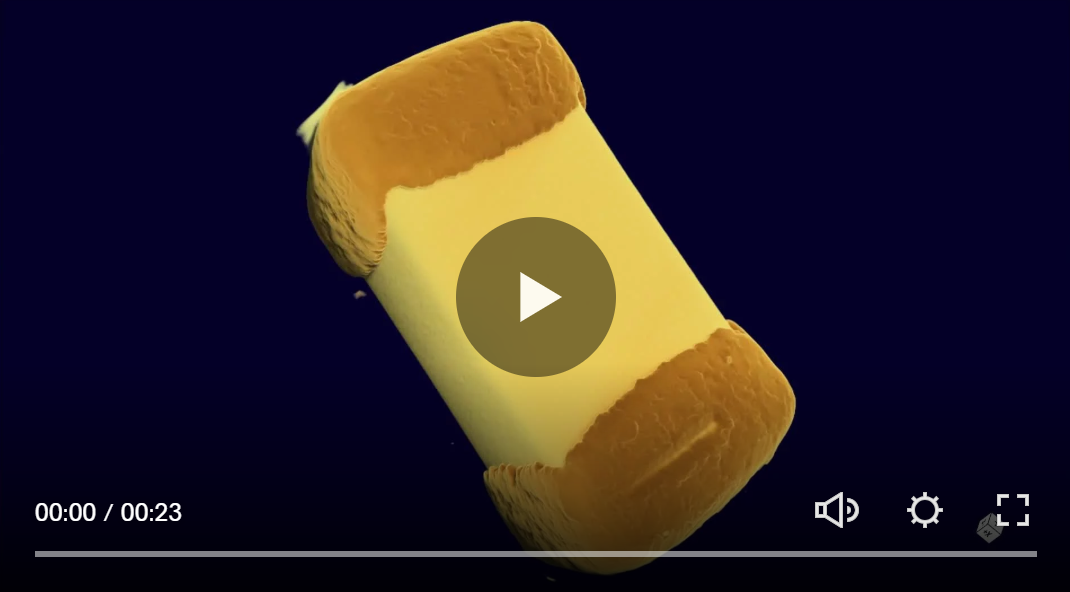
MLCC CT scan (video courtesy of Excillum)
Spectrum Logic detectors currently used in semiconductor and packaging inspection include: