
Many of our customers are pursuing 100% inline inspection for semiconductor packaging. The challenge is speed: CT scans of dense, miniature components such as chips and multi-layer ceramic capacitors (MLCCs) can take up to 10 minutes per part, making inline inspection impractical.
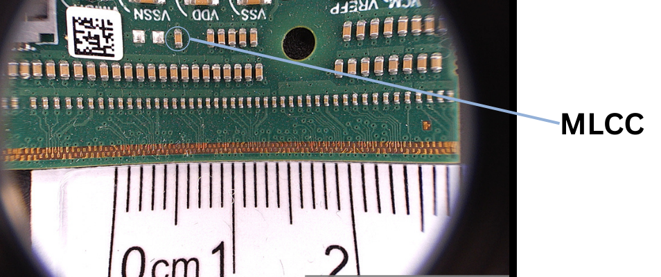
For a sense of scale - an MLCC on a sensor board viewed under a microscope
The solution is a detector that combines ultra-high resolution with high efficiency to enable much faster scanning. To meet this need, Spectrum Logic is developing the 6060XR (Extra Resolution) 10 µm CMOS Detector.
6060XR Features:
The 6060XR is a purpose-built detector for real-time X-ray imaging; featuring a 10 µm pixel pitch and a monolithic, stitched 60 × 60 mm² sensor with a novel ADC design. Users can select either a high-resolution Gadolinium oxide (Gd₂O₃) scintillator or a micro-columnar Caesium Iodide (CsI) scintillator.

6060XR layout
Key specifications:
Ultra-low read noise (<10 electrons) — versus ~100 electrons in standard CMOS and >1,000 in TFT-based detectors.
High spatial resolution without relying on extreme geometric magnification, minimizing artifacts in fine 3D structures.
Compact design that supports real-time inspection and high-resolution CT.
This innovation will enable next-generation CT scanners for advanced 3D semiconductor packaging, including high-bandwidth memory (HBM) used in AI chips. HBM stacks multiple DRAM layers to deliver high-speed data transfer and low power consumption—but requires precise X-ray imaging to inspect the microscopic interconnections between layers.
“The 6060XR will be a unique detector designed specifically for high-resolution X-ray imaging of advanced semiconductor packaging. This innovation will help manufacturers control quality and yield in advanced packaging, including GPU for AI applications and other cutting-edge semiconductor technologies.”
— Ed Bullard, Chairman, Spectrum Logic
*(In development)
IF you want more information on this product contact us on inquiries@spectrumlogic.com