

Spectrum Logic exhibited at Control 2023 - 9-12 May. Location: Hall 3 Booth 3601-1. Venue: Messe Stuttgart, Messepiazza 1, 70629 Stuttgart, Baden-Wurttemberg, Germany.

Advantages of CMOS for non-destructive testing (NDT)
Spectrum Logic has developed a range of X-ray detectors based on radiation hardened CMOS sensors for Industrial non-destructive testing with active area from 60 × 54 mm2 to 310 × 307 mm2, 50 and 100 μm pixel pitch.

They are ideally suited for industrial applications such as:
• 3D CBCT
• casting and electronics inspection
• metrology and material science
• weld and pipeline inspection
What is non-destructive testing?
Non-destructive testing (NDT) (also known as non-destructive inspection (NDI) and non-destructive Evaluation (NDE) is a process by which manufacturers look to detect, analyse and measure hidden faults and flaws. This inspection process aims to test products without destroying them. Using X-ray in NDT manufacturers are able to look for contaminants, defects and misaligned parts and are able to test and inspect connecting elements such as large metal castings, welded joints and assemblies without damaging or breaking the part being inspected.
As manufacturing has grown in scale so has the focus on product quality and safety. Ensuring the validity of components in the automotive and aerospace industries is essential. Failures in the field can be associated with enormous financial costs and damage to a manufacturer’s reputation. To prevent such problems arising quality standards have become increasingly demanding calling for 100% inspection of all parts.
Why is CMOS a wise choice of detector technology for X-ray NDT?
HIGH SPEED IMAGING
Due to the high electron mobility of crystalline silicon and our high-speed electronics, Spectrum Logic CMOS detectors achieve high frame rate over the full active area and at full resolution, reaching frame rates of >100 fps at full resolution. Higher frame rates are possible in ROI modes. Our detectors are free of image lag generated in the sensor and electronics although scintillators do generate some afterglow.
LOW NOISE AND HIGH RESOLUTION
Spectrum Logic’s proprietary active pixel sensor designs ensure low read noise and excellent image quality even at low signal levels. The technology permits small and large pixels to be designed from <15 μm to 150 μm.
INNOVATIVE DESIGN
Our sensors employ radiation hard pixel designs, with adjustable saturation dose, allowing the sensor to be used for high or low radiation levels, making our detectors suitable for a wide range of industrial NDT applications.
HIGH IMAGE QUALITY
CMOS FPDs have a higher readout speed and lower noise than a-Si and IGZO due to the much higher electrical charge mobility in crystalline silicon and the CMOS active pixel sensor (APS) architecture. Due to the low noise level of CMOS, the low dose Detective Quantum Efficiency (DQE) is significantly improved and X-ray detection is achieved even at very low dose levels.
LIFETIME DURABILITY
Our CMOS detector design has built-in radiation hardness both in the active pixel design and by virtue of the use of FOPs, which shield and protect the sensors and electronics. This design significantly improves the product reliability and enables a long operating life. For a superior image quality with high resolution for non-destructive testing imaging, CMOS (complementary metal-oxide semiconductor) flat panel detector.
AUTOMATIC EXPOSURE DETECTION
Spectrum Logic has developed advanced automatic exposure detection which is made possible by the CMOS active pixel technology used. The advanced, highly sensitive AED uses the entire sensor active area and responds to the onset of X-ray flux in 15 ms. Thanks to the low noise sensor and electronics, false triggers do not occur.
Why choose Spectrum Logic CMOS X-ray detectors?
KEY FEATURES:
• Broad product portfolio: active area from 60 × 54 mm mm2 to 310 × 307 mm2, 50 μm and 100 μm pixel pitch
• Fibre Optic Plate (FOP) – protects the sensor from radiation damage and reduces noise• Rad hard image sensor design
• High frame rates
• Automatic Exposure Detection (AED)
• Lower noise than aSi, IGZO or passive pixel CMOS
• Dual gain modes
• ROI modes with increased frame rates
• Scintillator can be customised to optimise the detector for the customer’s application
• No measurable image lag from CMOS sensor
• 5 GigE available, 10 GigE 1Q 2023
Case Study: Cabinet NDT

Electronics Inspection - Ball Grid Arrays
CMOS detectors offer small pixel size for higher spatial resolution to detect small features – such as broken wires and ball grid array defects. CMOS detectors have low image lag for a clearer image whether in real-time radiography or CT reconstruction. They also offer fast frame rates which are useful for inline inspection e.g. inline battery CT where high through-put is important.

Battery Inspection
CASE STUDY: Portable NDT: Heat Exchanger Inspection

Spectrum Logic has developed a thin 15010HS detector which has an industry leading thickness of 9mm, making it ideal for imaging hard to access objects such as heat exchangers.
To see the full portfolio download our CMOS X-ray detectors for NDT here or see our products here or contact us for further information.
Which technology will win the race to replace Image Intensifiers in the surgical C-arm market?
Over the past fifteen years, the surgical C-arm market has progressively transitioned from image intensifier (II)–based systems to flat panel detector (FPD) technologies. For many decades, X-ray imaging in C-arms relied on radiology imaging units (RIUs) composed of an image intensifier tube coupled to a charge-coupled device (CCD) camera assembly.
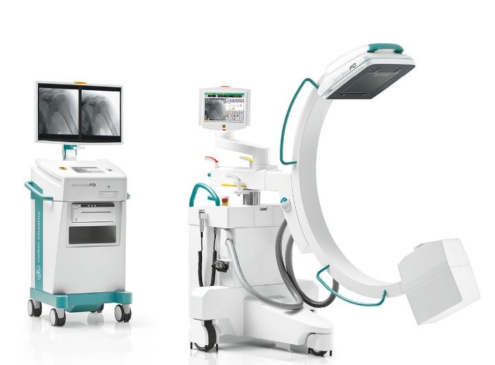
Image CMOSline C-arm courtesy of Ziehm Imaging
The shutdown of image intensifier manufacturing facilities1 and the growing clinical demand for advanced capabilities, including three-dimensional imaging, have accelerated the replacement of II–CCD RIUs in dynamic X-ray applications. Consequently, system manufacturers have increasingly adopted flat panel detectors and investigated alternative detector technologies. To date, three principal FPD technologies have emerged in the surgical C-arm domain: amorphous silicon (a-Si), indium gallium zinc oxide (IGZO), and complementary metal-oxide semiconductor (CMOS).
Advantages and weaknesses of a-Si, IGZO, and CMOS in the surgical C-arm market, and which technology is likely to lead
a-Si
Amorphous silicon (a-Si) is the non-crystalline form of silicon widely used in solar cells and thin-film transistors (TFTs) for flat-panel liquid crystal displays (LCDs) and televisions. Over the past two decades, a-Si flat-panel detectors (FPDs) have become the dominant technology in medical and industrial X-ray imaging. They are used in both static and dynamic imaging, although their largest application remains static general radiography, such as diagnostic orthopaedic imaging and chest X-ray.
Advantages of a-Si:
A-Si benefits significantly from its close ties to the display industry, where production occurs at extremely high volumes in large manufacturing facilities known as “fabs.” The latest Generation 10.5 a-Si display fabs use very large glass substrates measuring up to 2940 × 3370 mm, compared with the 200 mm or 300 mm silicon wafers typically used in CMOS fabs. As a result, a-Si FPDs enjoy strong economies of scale.
Most a-Si image sensors are manufactured in large display fabs in Asia, often repurposing older fabs that are no longer competitive for high-end consumer displays. This further reduces manufacturing costs, making a-Si a particularly cost-effective solution for large-area detectors, such as the 430 × 430 mm panels commonly used in chest X-ray imaging. In addition, a-Si FPDs tolerate high radiation doses well and offer a higher saturation dose than image intensifiers (IIs).
Disadvantages of a-Si:
Despite these advantages, a-Si performs poorly at low radiation doses due to relatively high read noise and slower pixel readout compared with II and CMOS technologies. The slow readout speed limits the achievable frame rate and prevents the use of small pixel sizes (for example, 100 μm) in high-frame-rate dynamic imaging. As a result, a-Si struggles to deliver both the speed required for fluoroscopy and the high spatial resolution needed for demanding applications such as cochlear implant procedures.
Even when larger pixels are used, the performance of current a-Si FPDs is constrained by the properties of a-Si TFTs. The low electron mobility of a-Si necessitates large TFT structures with high parasitic data-line capacitance, which in turn increases electronic noise. This noise is sufficiently high to significantly degrade image quality in low-dose fluoroscopy.2.
The relatively high electronic noise of a-Si detectors is their most significant limitation. Compared with IIs and CMOS detectors, a-Si systems require higher radiation doses to achieve acceptable image quality, increasing exposure for both patients and clinicians. This is a critical concern in the surgical C-arm environment, where clinicians may be exposed repeatedly. A study published in the American Journal of Roentgenology reported elevated risks of brain cancer, breast cancer, and melanoma among technologists performing fluoroscopically guided interventional procedures3. Consequently, reducing radiation exposure remains a key objective for C-arm manufacturers.
Another drawback of a-Si is image lag, which is undesirable in both fluoroscopy and 3D CT imaging. Although this effect can be partially mitigated through real-time image correction algorithms, it remains an inherent limitation of the technology.
IGZO
Another drawback of a-Si is image lag, which is undesirable in both fluoroscopy and 3D CT imaging. Although this effect can be partially mitigated through real-time image correction algorithms, it remains an inherent limitation of the technology.
Advantages of IGZO:
IGZO TFTs have an electron mobility that is <10x higher than a-Si2, which facilitates a reduction in the size of the TFT while also reducing the pixel discharge time. This results in an increase in the detector readout speed. Improving the readout speed is particularly important in achieving adequate frame rates in dynamic detectors with a pixel pitch of around 100 μm.
Because IGZO TFTs can be fabricated with smaller geometries than a-Si TFTs, they offer superior switching performance and improved pixel sensitivity. This enables faster readout and higher achievable detector resolution. Like a-Si, IGZO detectors are manufactured in large display fabs and benefit from similar economies of scale, with medical detector formats ranging from approximately 150 × 150 mm to 430 × 430 mm.
In terms of imaging performance, IGZO detectors occupy a middle ground between a-Si and CMOS. In low-dose fluoroscopy, IGZO systems can achieve usable image quality at equal or lower X-ray dose than a-Si, while supporting higher frame rates and improved resolution. However, their performance remains below that of CMOS detectors, particularly in very low-dose applications.
Disadvantages of IGZO
While IGZO offers clear performance improvements over a-Si, it does not yet match the low noise and high-speed performance of CMOS detectors. Manufacturers position IGZO as a lower-cost alternative to CMOS, making it an attractive replacement for image intensifiers and a-Si detectors in certain applications.
However, IGZO-based flat-panel detectors remain relatively immature. The technology has yet to demonstrate long-term reliability under sustained X-ray exposure in surgical C-arm environments. IGZO is less tolerant of X-ray radiation than a-Si and is therefore unsuitable for industrial radiography, raising concerns about detector lifetime in medical applications.
A 2019 report by Yole Development noted that while IGZO has long been viewed as a “high-performance, low-cost” TFT technology, a key challenge remains supply-chain readiness. Although multiple display manufacturers have begun offering IGZO panels for X-ray imaging, the technology does not yet match the production maturity, field experience, and proven reliability of a-Si or CMOS detectors.
IGZO detectors also exhibit some degree of image lag, although typically less than that observed with a-Si. As with other flat-panel technologies, image lag is undesirable in fluoroscopy and 3D CT imaging and represents an additional limitation.
CMOS
CMOS (complementary metal-oxide semiconductor) is the semiconductor technology used in most of today's computer microchips and image sensors. CMOS image sensors (CIS) are used in mobile phone cameras, compact cameras, video cameras and numerous machine vision applications. CMOS flat panel detectors for surgical C-arms were first launched in 2009 by the UK company Dexela (subsequently acquired by the US company PerkinElmer Inc) and introduced in mini C-arms the following year. CMOS was first used in full sized C-arms in 2017 with the launch of CMOS products by Ziehm Imaging and GE Healthcare. The technology has seen a strong level of growth in the dynamic X-ray imaging market, taking close to 100% of the mini C-arm market and most of the full sized C-arm market in developed economies. IIs still play an important role in the surgical C-arm market, especially in developing economies.
Advantages of CMOS
CMOS FPDs have a higher readout speed and lower noise than a-Si and IGZO due to the much higher electrical charge mobility in crystalline silicon and the CMOS active pixel sensor (APS) architecture. By lowering the noise floor, the low dose Detective Quantum Efficiency (DQE) is significantly improved and X-ray detection is achieved even at very low dose levels. CMOS FPDs are able to simultaneously yield better resolution and better contrast for the highest diagnostic image quality available. This results in a reduction of radiation dose to the patient and clinicians in low dose fluoroscopy in comparison with a-Si detectors.
CMOS image sensor technology also allows multiple gain modes to be implemented at the pixel level allowing different modes of operation for high dose and low dose applications, such as 3D CT imaging (high dose) and low dose fluoroscopy.
CMOS image sensors have virtually no image lag in the sensor itself, although the scintillator layer that converts X-ray photons into visible light does have some afterglow.
Disadvantages of CMOS
While CMOS detectors have the best performance characteristics (including resolution, speed and low dose image quality), the cost of the CMOS sensors results in a high cost for larger panels, e.g. 310 mm2. This is due to the relatively high cost of CMOS wafers compared to a-Si or IGZO image sensors.
Although CMOS image sensors are vulnerable to radiation damage by X-rays, CMOS X-ray detectors used in surgical C-arms are protected by a fibre optic plate (FOP), which adds additional cost but improves image quality and product lifetime.
Conclusion
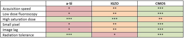
As we can see in the table below CMOS has significant advantages in the race to replace IIs in the C-arm market and is the clear winner for high performance systems whereas IGZO and a-Si have a cost advantage for value systems. (***=best in class)
1. In the last 6 years we have witnessed ON Semiconductor, formerly Kodak closing one of its CCD factories, prior to that Sony’s CCD operations were also shut down. Argus Imaging and Thales have also stopped manufacturing image intensifiers.
2. ‘Analysis of a new indium gallium zinc oxide (IGZO) detector’, Steven Freestone, Richard Weisfield, Carlo Tognina, Isaias Job, Richard E. Colbeth.
3. Rajaraman, P. et al. (2016) ‘Cancer Risks in U.S. Radiologic Technologists Working With Fluoroscopically Guided Interventional Procedures, 1994-2008’, AJR. American journal of roentgenology, 206(5), pp. 1101–1108; quiz 1109. doi:10.2214/AJR.15.15265.
4. ‘Mobile C-Arm with a CMOS Detector: Technical Assessment of Fluoroscopy and Cone-Beam CT Imaging Performance’, Niral M. Sheth, Wojciech Zbijewski, Matthew W. Jacobson, Godwin Abiola, Gerhard Kleinszig, Sebastian Vogt, Stefan Soellradl, Jens Bialkowski, William S. Anderson, Clifford R. Weiss, Greg M. Osgood, and Jeffrey H. Siewerdsen.

Spectrum Logic to exhibit at ASNT Annual Conference in Nashville, October 2022
The Spectrum Logic team are exhibiting at the American Society of Nondestructive Testing (ASNT) Annual Conference in Nashville. We will be presenting our CMOS flat panel detectors (FPDs) for NDT. Booth #646
Mon 31 Oct – Thu 3 Nov
Gaylord Opryland Resort & Convention Center, 2800 Opryland Dr, Nashville, TN, United States
Email us at inquiries@spectrumlogic.com if you want to set up a meeting at the exhibition.
Download our data sheet about CMOS Detectors for Non-Destructive Testing.
