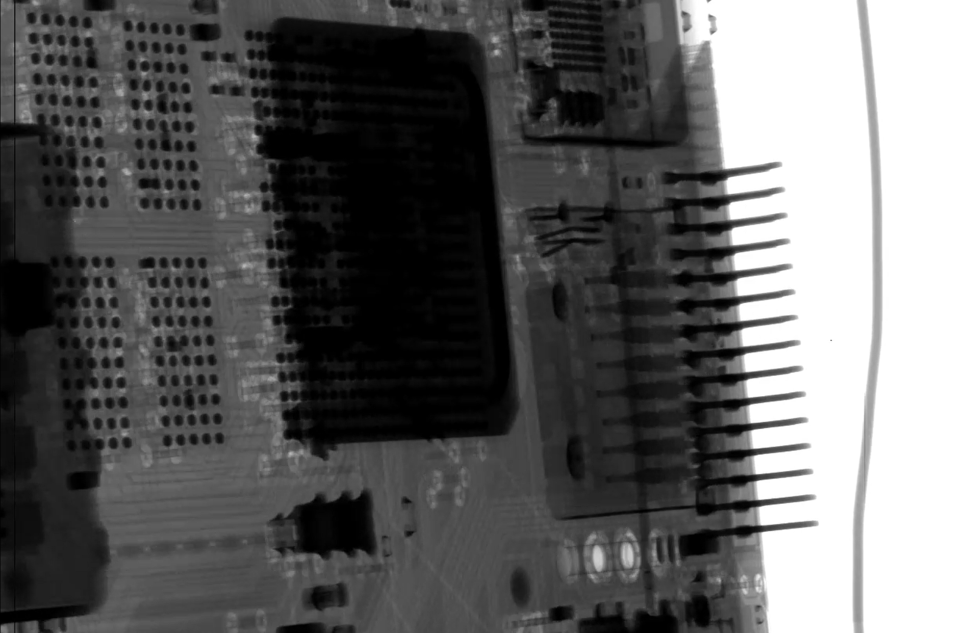
AXI

What type of X-ray detector is best for PCB inspection?

What type of X-ray detector is best for PCB inspection?

Automated PCB X-ray inspection is an important quality control technology using either 2D or 3D X-ray imaging to detect defects in products during the production process. AXI complements automated optical inspection (AOI) by detecting defects that are invisible to optical cameras such as voids in ball grid arrays (BGAs), widely used in surface mount packaging. Different types of X-ray detector can be used for the automated inspection of PCBs, but which type is the best suited to the task?

Read More

Why are large area CMOS X-ray detectors with radiation tolerant FOPs the best choice for AXI in electronics manufacturing?

Automated X-ray inspection (AXI) is an industrial inspection modality based on the same principles as automated optical inspection (AOI). The object of inspection is illuminated with X-rays in AXI, whereas AOI uses illumination with visible light. Both AXI and AOI automatically inspect features of products such as printed circuit boards (PCB) to detect defective products in the production process. AXI has the unique ability to detect faults that are hidden from view and cannot be detected by AOI. The classic example of a fault in a PCB is a defect in ball-grid array (BGA), a packaging technology used for surface-mount packaging for integrated circuits on PCBs. The BGA’s bottom surface is an array of pads with balls of solder. These connections need to be carefully soldered due to their location which prevents visual inspection. Common defects in BGAs include misalignment, inconsistent standoff height, non-wetted pads, bridges, partial reflow, popcorning (when balls merge together during soldering), missing balls and the presence of voids in balls.

Automated X-ray inspection is used both to detect defects, which can be scrapped or reworked, and for process optimization, in which the results of the inspection provide feedback to allow the production process to be optimised. For example, an electrical test can identify an open circuit but it cannot identify the cause of the issue, which would allow the root cause of the defect in the production process to be identified and fix.

3D CT AXI images

Both AOI and AXI are widely used in inline role electronics manufacturing for PCBs but also for power modules, connectors and other components. Inline AXI tests all pieces manufactured by a production line rather than testing samples or defective pieces identified with another method. High throughput is a key requirement for AXI as well as good image quality and reliability.  In recent years 3D computed tomography (CT) or types of limited-angle CT known as tomosynthesis have become common in AXI because they provide more information about the object of inspection and avoid the risk of defects being concealed by overlapping structures. The task of performing CT or tomosynthesis on objects in a few seconds, to allow high throughput, is a difficult one and requires both a relatively high X-ray flux and a high-speed, high-resolution detector. To image larger PCBs or other components a large active area is also required.

The fastest large area CMOS detectors available today for industrial applications is the Spectrum Logic 2824HS, which has 100 µm pixel pitch, an active area of 280 x 240 mm2 and a frame rate of 90 fps with a 10 Gigabit Ethernet (GigE) interface and 170 fps at 50% region of interest (ROI) mode. This is three times fast than competing detectors and has been adopted for high-end AIX. The Spectrum Logic 3131HS, also has 100 um pixel pitch and has the largest active area of any dynamic CMOS X-ray detector of 309 x 307 mm2. It has a maximum readout speed of 62 fps with 10 GigE in full frame mode and offers faster region of interest modes.

Another advantage of CMOS technology for AIX is the reduction in image lag in comparison with competing amorphous silicon (a-Si) flat panel X-ray detectors. This improves the image quality of 3D reconstructions by preventing images being mixed with fading copies of previous images.

Reliability and lifetime are also important considerations. Image sensor and other semiconductors are damaged by ionising radiation such as X-rays. X-ray detectors can, therefore, be damaged by the X-ray flux they are detecting. While detector electronics can be shielded from X-rays with lead or other shielding materials, the imaging active area cannot. Spectrum Logic’s detectors get around they problem by using special fibre optic faceplates (FOPs) between the scintillator and the CMOS image sensor array to block X-rays but transmit the image produced by the interaction of the scintillator with the X-ray beam. Spectrum Logic’s detectors use a specialised cerium doped glass for industrial FOPs to avoid browning of the glass through X-ray radiation. The combination of radiation hard CMOS image sensor design and thick radiation tolerant FOPs gives an extended detector lifetime and enhanced reliability. 

What is inside a Spectrum Logic X-ray detector

Inside a Spectrum Logic CMOS X-ray Detector

By using a large area CMOS X-ray detector, CT or tomosynthesis systems can process 10 parts per minute or more with excellent image quality and defect detection capability.